

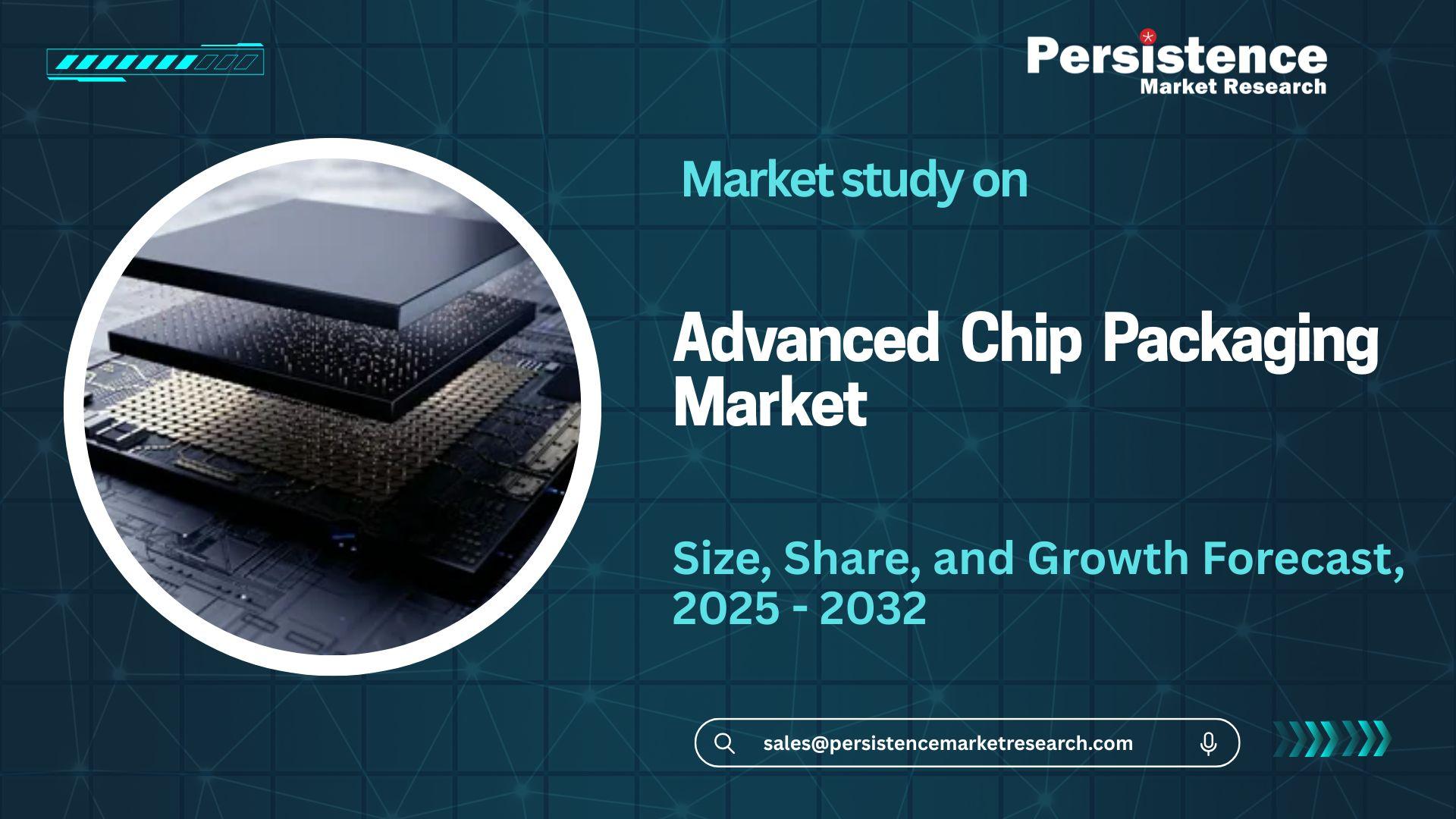
Advanced Chip Packaging Market Insights Growth Drivers and Industry Forecast
The global advanced chip packaging market is undergoing a remarkable transformation, driven by the surging demand for high-performance semiconductors in a wide range of applications. The integration of artificial intelligence, 5G, and the Internet of Things has created a pressing need for advanced semiconductor devices that deliver enhanced performance, higher efficiency, and miniaturization. As electronic devices continue to shrink in size while increasing in functionality, chip packaging plays a crucial role in supporting these innovations. Advanced packaging techniques allow multiple components to be integrated efficiently, improving power management, reducing latency, and enhancing thermal performance.
According to Persistence Market Research, the global advanced chip packaging market is forecast to expand at a compound annual growth rate of 19.7 percent, growing from an expected value of US$16 billion in 2024 to US$56.6 billion by the end of 2031. This remarkable growth trajectory reflects the strong demand for advanced packaging technologies and the increasing adoption of complex semiconductors across industries.
Advanced chip packaging is more than a simple protective casing for microchips. It involves intricate engineering that allows the integration of multiple semiconductor dies, passive components, and interconnections into a single package. The technology addresses challenges in signal integrity, thermal management, and device reliability, which are essential as computing power requirements increase. With the proliferation of AI, machine learning, and high-speed data communication technologies, the demand for advanced packaging solutions is set to rise rapidly.
Market Segmentation
The advanced chip packaging market can be categorized into several segments, including packaging type, application, and end-user industry. Each segment highlights the versatility and range of applications of advanced packaging technologies.
By Packaging Type
- 2.5D Packaging: 2.5D packaging involves placing multiple dies side by side on an interposer, which enables high-density interconnections and enhanced performance. This method is particularly useful in networking and data center applications where bandwidth and processing speed are critical.
- 3D Packaging: 3D packaging stacks semiconductor dies vertically, significantly reducing the footprint while improving performance by minimizing the length of interconnects. It is widely used in high-performance computing, mobile devices, and memory-intensive applications.
- System-in-Package (SiP): SiP integrates heterogeneous components such as processors, memory, and sensors into a single package. This approach is essential for wearables, smartphones, and IoT devices, offering compactness without compromising functionality.
- Fan-Out Wafer-Level Packaging (FOWLP): FOWLP extends the interconnects beyond the wafer’s edge, allowing more input/output connections and better thermal and electrical performance. It is increasingly adopted in smartphones, automotive electronics, and consumer devices.
By Application
- Consumer Electronics: Smartphones, tablets, wearables, and gaming devices rely heavily on advanced chip packaging to meet performance and power efficiency requirements. Devices are expected to become more compact and energy-efficient, driving demand for multi-chip integration.
- Automotive: The automotive sector increasingly relies on semiconductor devices for electric vehicles, autonomous driving systems, and advanced driver-assistance systems. These applications require robust and reliable packaging solutions that can withstand high temperatures, vibrations, and harsh environmental conditions.
- Telecommunications: The deployment of 5G infrastructure and the rising demand for high-speed data networks are fueling the need for advanced chip packaging. Base stations, network routers, and other telecom devices require high-performance semiconductors with enhanced thermal and electrical management.
- Industrial Electronics: Industrial automation, robotics, and manufacturing systems are leveraging advanced semiconductor technologies to improve efficiency and reliability. Advanced packaging ensures that chips perform optimally under demanding operational conditions.
By End-User Industry
- Semiconductor Manufacturers: Chip manufacturers are the primary adopters of advanced packaging solutions. Leading semiconductor firms integrate packaging technologies into their production to improve performance and enhance product differentiation.
- Original Equipment Manufacturers (OEMs): OEMs utilize advanced packaging in the development of end-user devices. These companies focus on high-performance products that meet consumer expectations for compactness and efficiency.
- Research and Development Institutions: Academic and industrial research centers are working on the next generation of advanced packaging technologies. Their innovations aim to overcome material limitations, improve thermal management, and support higher integration density.
Key Drivers of Market Growth
The advanced chip packaging market is being propelled by several interrelated factors:
- Technological Advancements: Innovations such as through-silicon vias, hybrid bonding, and micro-bump interconnects are enabling higher performance and smaller chip sizes. Continuous R&D ensures that packaging solutions meet the needs of next-generation electronics.
- Increasing Demand for AI and 5G: AI-enabled devices and 5G infrastructure require high-speed, high-efficiency chips. Advanced packaging allows manufacturers to integrate multiple dies and improve thermal management, supporting faster processing and data transfer.
- Miniaturization Trends: Consumer preference for compact and multifunctional devices continues to grow. Advanced chip packaging allows multiple components to coexist in smaller form factors, enabling sleeker and more portable devices.
- Cost Efficiency and Yield Improvement: Advanced packaging can improve yield and reduce production costs by simplifying the integration of complex systems into a single package. This economic advantage is attracting semiconductor manufacturers.
Challenges Facing the Market
Despite the favorable growth prospects, the market faces several challenges:
- Complex Manufacturing Processes: Advanced packaging requires precise manufacturing and specialized equipment, which can be costly and time-consuming to implement.
- Material Limitations: The development of high-performance materials that can sustain thermal and electrical demands is essential. Limited availability of such materials may constrain growth.
- Supply Chain Constraints: Availability of raw materials, components, and advanced manufacturing tools can affect production timelines and costs, particularly during global disruptions.
- Environmental Concerns: Packaging materials and processes must comply with environmental regulations. The industry is moving toward sustainable and recyclable packaging solutions, but this adds to the cost and complexity of production.
Regional Insights
The advanced chip packaging market varies significantly across regions due to the presence of major manufacturers, technological capabilities, and industrial demand.
- North America: The United States is a major player in the advanced chip packaging market, supported by domestic semiconductor manufacturers and large-scale investments in research and production facilities. The region benefits from government initiatives to promote chip manufacturing and innovation in packaging technologies.
- Asia-Pacific: Taiwan, South Korea, and Japan lead the global advanced packaging market. Companies in these countries are at the forefront of innovations such as 3D stacking and fan-out wafer-level packaging. Taiwan’s ASE Technology Holding Co., for example, expects revenue from advanced packaging and testing to rise significantly from 2024 to 2025, reflecting the region’s technological edge.
- Europe: European semiconductor companies are focusing on developing advanced packaging to support high-performance electronics. Firms like BE Semiconductor Industries are increasing long-term financial targets in response to growing demand for chip stacking and system-in-package solutions.
Key Players in the Market
Several major companies dominate the advanced chip packaging market globally:
- TSMC: Taiwan Semiconductor Manufacturing Company is a leader in 2.5D and 3D packaging technologies, serving clients across consumer electronics and high-performance computing.
- ASE Technology Holding Co.: ASE provides comprehensive packaging and testing services, including fan-out wafer-level packaging, system-in-package, and advanced interconnect solutions.
- Amkor Technology: Amkor specializes in wafer-level packaging, system-in-package, and advanced semiconductor assembly. The company is investing heavily in new manufacturing facilities to expand capacity.
- Intel Corporation: Intel leverages advanced packaging to develop high-performance processors and memory solutions, integrating multiple dies for better performance and efficiency.
- Samsung Electronics: Samsung’s semiconductor division is a significant player in advanced packaging, particularly in memory and mobile device applications.
- STATS ChipPAC: The company provides advanced packaging solutions including system-in-package, wafer-level packaging, and flip-chip technologies, serving various global clients.
- JCET Group: JCET is a key player in advanced packaging services, including wafer-level packaging and 3D IC integration.
Future Outlook
The advanced chip packaging market is expected to continue its rapid growth trajectory through 2031, driven by:
- Integration of Artificial Intelligence: AI applications require high-performance computing chips, increasing demand for 3D packaging, SiP, and high-density interconnect solutions.
- Development of Advanced Materials: New materials capable of handling high thermal loads and electrical performance are being developed, allowing chips to perform reliably in demanding applications.
- Sustainability and Green Packaging: Industry trends are moving toward environmentally friendly materials and processes, reducing the ecological impact of chip packaging.
- Expansion of Manufacturing Capabilities: Global semiconductor companies are investing in new manufacturing plants and production lines, increasing the availability of advanced packaging solutions to meet growing global demand.
Conclusion
The global advanced chip packaging market is set for substantial growth, expanding from US$16 billion in 2024 to US$56.6 billion by 2031 at a CAGR of 19.7 percent. The growth is driven by the increasing demand for high-performance semiconductors across AI, 5G, IoT, automotive, and consumer electronics applications. Advanced packaging solutions such as 3D packaging, system-in-package, and fan-out wafer-level packaging enable smaller, faster, and more energy-efficient devices.
While challenges such as complex manufacturing processes, material limitations, and supply chain constraints exist, ongoing technological innovations, investment in manufacturing capabilities, and sustainability initiatives are expected to mitigate these obstacles. Companies that invest in research and development, advanced manufacturing, and environmentally friendly solutions will gain a competitive advantage in this rapidly evolving market. The next decade promises exciting developments in advanced chip packaging, making it a critical component of the semiconductor ecosystem and a key enabler of next-generation electronic devices.